| CPC G06F 13/1668 (2013.01) [G06F 13/4022 (2013.01); G06F 13/4282 (2013.01); H01L 23/562 (2013.01); H01L 25/0657 (2013.01); H01L 25/18 (2013.01); H01L 2225/0652 (2013.01); H01L 2225/06513 (2013.01); H01L 2225/06517 (2013.01); H01L 2225/06541 (2013.01); H01L 2225/06586 (2013.01)] | 20 Claims |
|
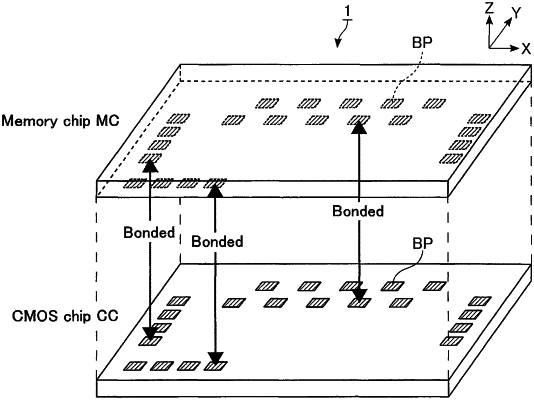
1. A memory system comprising:
a first chip including a first surface, the first chip including:
a memory cell array, and
a first bonding pad on the first surface, the first bonding pad being electrically coupled to the memory cell array; and
a second chip including a second surface, the second surface facing the first surface of the first chip, the second chip including:
a memory controller configured to control access to the memory cell array, and
a second bonding pad on the second surface, the second bonding pad being directly bonded with the first bonding pad of the first chip to be electrically coupled thereto, the second bonding pad further being electrically coupled to the memory controller.
|