| CPC G06F 11/1068 (2013.01) [G06F 11/0772 (2013.01); G06F 13/4068 (2013.01)] | 20 Claims |
|
1. A controller, comprising:
a processing circuit configured to:
write each data fragment of a plurality of data fragments in one memory chip of a plurality of memory chips, wherein
each data fragment of the plurality of data fragments includes a part of data to be written, and
each memory chip of the plurality of memory chips has an error correction function; and
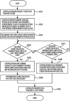
read the plurality of data fragments corresponding to data to be read from the plurality of memory chips;
a first encoder configured to encode the data to be written with an erasure correction code such that each data fragment of the plurality of data fragments includes a parity; and
a first decoder configured to perform erasure correction by use of a part of the plurality of data fragments corresponding to the data to be read according to a completion status of error correction on a corresponding part of the plurality of data fragments in each memory chip of the plurality of memory chips, wherein the completion status of the error correction is acquired via a signal line.
|