| CPC G06F 1/1656 (2013.01) [H01L 27/124 (2013.01)] | 19 Claims |

|
1. A display panel, comprising:
a first substrate; and
a second substrate opposite to the first substrate;
wherein the display panel is divided into a display area and a frame area located at a periphery of the display area;
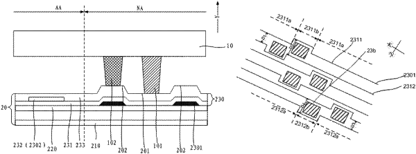
wherein a plurality of first main support columns and a plurality of auxiliary support columns are arranged in the frame area, and a length of each of the plurality of first main support columns is greater than a length of each of the plurality of auxiliary support columns in a light emitting direction of the display panel;
wherein the plurality of first main support columns are located on a side of the first substrate facing the second substrate;
wherein the second substrate comprises a base, a first surface and a second surface, the first surface and the second surface are located on a side of the second substrate facing the first substrate, and a height from the second surface to the base is greater than a height from the first surface to the base;
wherein orthographic projections of the plurality of first main support columns on the base are located within an orthographic projection of the first surface on the base,
wherein the second substrate comprises a planarization layer on a side of the base facing the first substrate, and a wiring layer on a side of the planarization layer facing the first substrate; and
wherein the wiring layer comprises a plurality of electrode leads in the frame area, orthographic projections of the plurality of electrode leads on the base are located within an orthographic projection of the second surface on the base, and the orthographic projection of the first surface on the base is located within an orthographic projection of a gap between adjacent electrode leads of the plurality of electrode leads on the base.
|