US 11,853,105 B2
SSD architecture for FPGA based acceleration
Ramdas P. Kachare, Pleasanton, CA (US); Fred Worley, San Jose, CA (US); Harry Rogers, San Jose, CA (US); Wentao Wu, Milpitas, CA (US); and Nagarajan Subramaniyan, San Jose, CA (US)
Assigned to SAMSUNG ELECTRONICS CO., LTD.
Filed by Samsung Electronics Co., Ltd., Suwon-si (KR)
Filed on Feb. 26, 2021, as Appl. No. 17/187,735.
Application 17/187,735 is a continuation of application No. 16/752,612, filed on Jan. 24, 2020, granted, now 11,132,310.
Application 16/752,612 is a continuation of application No. 16/122,865, filed on Sep. 5, 2018, granted, now 10,585,819, issued on Mar. 10, 2020.
Claims priority of provisional application 62/642,568, filed on Mar. 13, 2018.
Claims priority of provisional application 62/641,267, filed on Mar. 9, 2018.
Claims priority of provisional application 62/638,904, filed on Mar. 5, 2018.
Prior Publication US 2021/0182221 A1, Jun. 17, 2021
This patent is subject to a terminal disclaimer.
Int. Cl. G06F 13/16 (2006.01); G06F 13/40 (2006.01); G06F 13/42 (2006.01)
CPC G06F 13/1668 (2013.01) [G06F 13/4027 (2013.01); G06F 13/4282 (2013.01); G06F 2213/0026 (2013.01)] 20 Claims
OG exemplary drawing
 
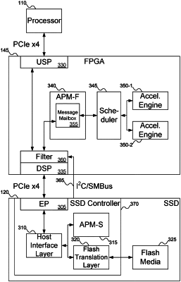
1. A system, comprising:
a first interface for communicating with a processor;
a second interface for communicating with a storage device;
an accelerator to execute an acceleration instruction, the accelerator implemented using hardware, the accelerator configured to send an instruction to the storage device based at least in part on the acceleration instruction; and
the storage device, including:
a port of the storage device for communicating with the accelerator;
a controller to manage operations of the storage device;
storage to store a data; and
a storage device acceleration manager to send the data to the accelerator based at least in part on the instruction,
wherein a storage instruction is transmitted from the first interface to the second interface.