US 11,852,977 B2
Apparatus and methods of electrically conductive optical semiconductor coating
Bradley Dean Schwartz, Brewster, NY (US)
Assigned to Danbury Mission Technologies, LLC, Colorado Springs, CO (US)
Filed by Danbury Mission Technologies, LLC, Colorado Springs, CO (US)
Filed on Mar. 22, 2021, as Appl. No. 17/208,958.
Application 17/208,958 is a division of application No. 16/166,788, filed on Oct. 22, 2018, granted, now 10,955,747.
Application 16/166,788 is a division of application No. 15/259,400, filed on Sep. 8, 2016, granted, now 10,126,656, issued on Nov. 13, 2018.
Prior Publication US 2022/0043355 A1, Feb. 10, 2022
This patent is subject to a terminal disclaimer.
Int. Cl. G03F 7/32 (2006.01); C23C 14/48 (2006.01); G02B 1/11 (2015.01); G02B 1/14 (2015.01); G03F 7/20 (2006.01); H01L 31/0216 (2014.01); H01L 23/552 (2006.01)
CPC G03F 7/32 (2013.01) [C23C 14/48 (2013.01); G02B 1/11 (2013.01); G02B 1/14 (2015.01); G03F 7/20 (2013.01); H01L 23/552 (2013.01); H01L 31/0216 (2013.01)] 20 Claims
OG exemplary drawing
 
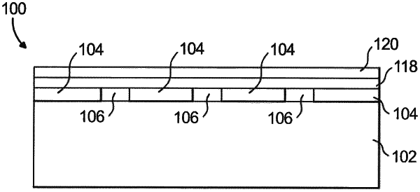
1. A window, comprising:
a transparent substrate;
a coating disposed over a portion of the transparent substrate, the coating comprising a first plurality of regions formed of a transparent semiconductor, and a second plurality of regions formed of an electrically conductive semiconductor.