US 11,852,966 B2
Lithography mask with a black border regions and method of fabricating the same
Chin-Hsiang Lin, Hsinchu (TW); Chien-Cheng Chen, Hsinchu County (TW); Hsin-Chang Lee, Hsinchu County (TW); Chia-Jen Chen, Hsinchu County (TW); Pei-Cheng Hsu, Taipei (TW); Yih-Chen Su, Taichung (TW); Gaston Lee, Hsinchu County (TW); and Tran-Hui Shen, Yunlin County (TW)
Assigned to TAIWAN SEMICONDUCTOR MANUFACTURING CO., LTD., Hsinchu (TW)
Filed by Taiwan Semiconductor Manufacturing Co., Ltd., Hsinchu (TW)
Filed on Jun. 7, 2021, as Appl. No. 17/340,991.
Application 16/660,300 is a division of application No. 15/851,829, filed on Dec. 22, 2017, granted, now 10,866,504, issued on Dec. 15, 2020.
Application 17/340,991 is a continuation of application No. 16/660,300, filed on Oct. 22, 2019, granted, now 11,029,593.
Prior Publication US 2021/0294203 A1, Sep. 23, 2021
This patent is subject to a terminal disclaimer.
Int. Cl. G03F 1/24 (2012.01); G03F 1/54 (2012.01); G03F 7/20 (2006.01); G03F 1/38 (2012.01); G03F 1/22 (2012.01)
CPC G03F 1/24 (2013.01) [G03F 1/38 (2013.01); G03F 1/54 (2013.01); G03F 7/2004 (2013.01); G03F 1/22 (2013.01)] 20 Claims
OG exemplary drawing
 
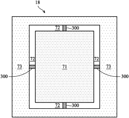
1. A lithography mask, comprising:
a substrate; and
a reflective structure located over the substrate;
wherein:
the lithography mask includes a first region, a second region that surrounds the first region in a top view, and a third region that surrounds the second region in the top view;
the second region includes a substantially non-reflective material;
a plurality of bridges are located in the second region;
each of the bridges is configured to diffuse electrical charges from the first region into the third region; and
the bridges each have a material composition that is different than a material composition of a remainder of the second region.