| CPC G02F 1/136286 (2013.01) [G02F 1/1339 (2013.01); G02F 1/1345 (2013.01); G02F 1/13452 (2013.01)] | 12 Claims |
|
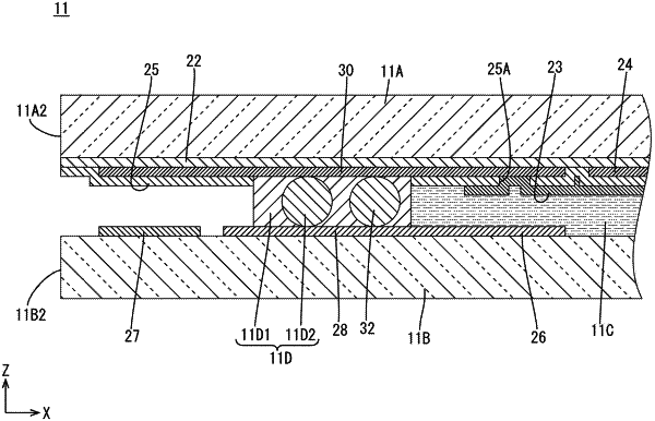
1. A display device comprising:
a first substrate including
a first line,
a second line disposed at a distance from the first line and extending in an extending direction and parallel to the first line,
a first connection electrode projecting from the first line toward the second line, and
a second connection electrode projecting from the second line toward the first line and being disposed such that the second connection electrode and the first connection electrode are arranged in the extending direction;
a second substrate disposed opposite the first substrate and including
a first electrode,
a third connection electrode that is electrically connected to the first electrode and disposed to overlap the first connection electrode,
a second electrode, and
a fourth connection electrode that is electrically connected to the second electrode and disposed to overlap the second connection electrode and disposed such that the fourth connection electrode and the third connection electrode are arranged in the extending direction;
a first electrically conductive portion disposed between the first substrate and the second substrate to overlap the first connection electrode and the third connection electrode, the first electrically conductive portion being contacted with the first connection electrode and the third connection electrode; and
a second electrically conductive portion disposed between the first substrate and the second substrate to overlap the second connection electrode and the fourth connection electrode, the second electrically conductive portion being contacted with the second connection electrode and the fourth connection electrode.
|