| CPC G02F 1/136286 (2013.01) [G02F 1/1368 (2013.01)] | 12 Claims |
|
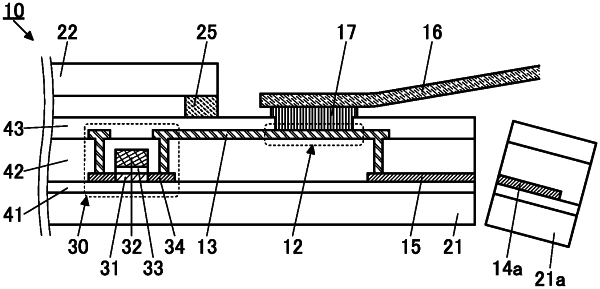
1. A display device comprising a substrate, a display portion, a first wiring, and a second wiring,
wherein the display portion comprises a transistor,
wherein the transistor comprises a semiconductor layer, a gate insulating layer, and a gate electrode,
wherein the semiconductor layer at least comprises one metal element that is the same as the metal element included in the second wiring,
wherein the semiconductor layer comprises a first region overlapping with the gate electrode and a second region not overlapping with the gate electrode,
wherein the second wiring and the second region of the semiconductor layer are electrically connected by the first wiring, and
wherein a resistance of the second region and a resistance of the second wiring are lower than a resistance of the first region.
|