| CPC G02F 1/136263 (2021.01) [G02F 1/136295 (2021.01); H01L 22/22 (2013.01); H01L 27/1244 (2013.01)] | 20 Claims |
|
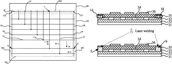
1. A display panel, comprising a display region and a non-display region positioned at a side of the display region, wherein the display region comprises:
a plurality of gate lines extending laterally;
at least one gate repair line;
a plurality of gate connection lines extending longitudinally to the non-display region; and
at least one first connection repair line extending longitudinally;
wherein the at least one gate repair line is connected to the at least one first connection repair line in a one-to-one correspondence, each of the at least one gate repair line is provided with a plurality of first connection repair points positioned in one-to-one correspondence with the gate connection lines, and each of the first connection repair lines is provided with a plurality of second connection repair points positioned in one-to-one correspondence with the gate lines.
|