| CPC G02F 1/136254 (2021.01) [G02F 1/136259 (2013.01); G02F 1/136263 (2021.01); G02F 1/136286 (2013.01); G02F 1/136222 (2021.01)] | 19 Claims |
|
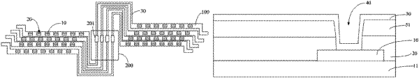
1. A shorting bar, comprising a plurality of test lines, wherein each of the test lines comprises:
a base substrate;
an insulation layer disposed on the base substrate, wherein one or more via holes are defined in the insulation layer;
one or more metal wires disposed in the insulation layer, wherein each of the metal wires are at least partially exposed in one of the via holes;
a conductive layer at least partially disposed in the via holes and covering the exposed metal wires, wherein the conductive layer is a strippable conductive layer; and
a test pad connected to the test lines, wherein the test pad comprises a plurality of test sub-pads that are disposed in a spaced manner.
|