| CPC G02F 1/136222 (2021.01) [G02F 1/136286 (2013.01)] | 21 Claims |
|
1. A liquid crystal display device comprising:
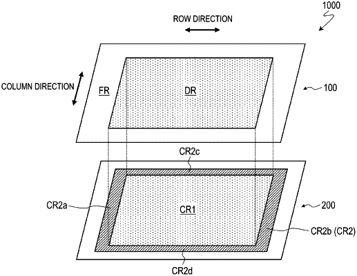
a first liquid crystal panel including a display region and including a color filter layer;
an illumination device provided on a back face side of the first liquid crystal panel; and
a second liquid crystal panel arranged between the first liquid crystal panel and the illumination device and not including a color filter layers;
wherein the second liquid crystal panel includes:
a first dimming region defined by a plurality of pixels arranged in a matrix including a plurality of rows and a plurality of columns and facing the display region; and
a second dimming region defined by a plurality of additional pixels each including an unshaded opening region and located outside the first dimming region;
the second liquid crystal panel includes a plurality of gate wiring lines extending in a row direction and a plurality of source wiring lines extending in a column direction;
the second dimming region includes a first portion and a second portion that extend in the column direction and are arranged sandwiching the first dimming region in the row direction;
the liquid crystal display device further includes a source wiring line drive circuit configured to supply source signals to the plurality of source wiring lines;
the plurality of source wiring lines include a plurality of first source wiring lines provided corresponding to the plurality of pixels and a plurality of second source wiring lines provided corresponding to additional pixels located in the first portion and the second portion of the second dimming region among the plurality of additional pixels;
the source wiring line drive circuit includes a plurality of source output terminals each configured to output a source signal and outnumbering the plurality of source wiring lines; and
the plurality of source output terminals include a plurality of first source output terminals electrically connected to the plurality of first source wiring lines, a plurality of second source output terminals electrically connected to the plurality of second source wiring lines, and a plurality of third source output terminals not electrically connected to either the plurality of first source wiring lines or the plurality of second source wiring lines.
|