| CPC G02F 1/13452 (2013.01) [G02F 1/13458 (2013.01); G02F 1/133345 (2013.01); G09G 3/3696 (2013.01); H05K 1/118 (2013.01); H05K 1/189 (2013.01); G09G 2300/0426 (2013.01); G09G 2300/0478 (2013.01); G09G 2310/0278 (2013.01); H05K 2201/09236 (2013.01); H05K 2201/10128 (2013.01); H05K 2201/10136 (2013.01)] | 20 Claims |
|
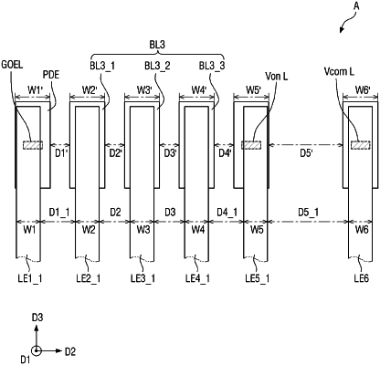
1. A display device comprising:
a display panel including a plurality of connecting signal wires which supply different control voltages controlling the display panel and at least one bump wire which is disposed between adjacent connecting signal wires not to overlap any one of the plurality of connecting signal wires in a plan view, the at least one bump wire being not supplied with the different control voltages controlling the display panel, the display panel including a top surface through which an image is displayed, a bottom surface opposing the top surface and a side surface connecting the top surface and the bottom surface;
a flexible printed circuit board attached to the side surface of the display panel and including a base film and a plurality of lead wires which are disposed on the base film; and
an anisotropic conductive film disposed between the plurality of connecting signal wires and the plurality of lead wires,
wherein the plurality of connecting signal wires and the at least one bump wire are disposed on a same plane in the display panel.
|