| CPC G02F 1/134363 (2013.01) [G02F 1/1337 (2013.01); G02F 1/1368 (2013.01); G02F 1/13306 (2013.01); G02F 1/133707 (2013.01); G02F 1/136286 (2013.01); G02F 1/13373 (2021.01); G02F 1/134381 (2021.01); G02F 1/136227 (2013.01); G02F 2201/122 (2013.01); G02F 2201/123 (2013.01); G02F 2201/128 (2013.01)] | 14 Claims |
|
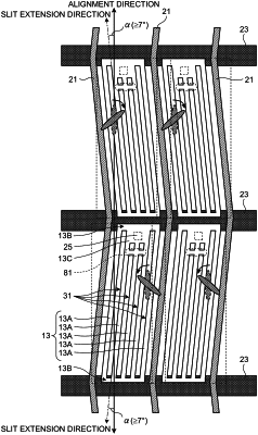
1. A display device comprising:
a substrate;
a first pixel with a first electrode on the substrate;
a second pixel with a second electrode on the substrate, the first pixel being adjacent to the second pixel;
a first scanning line between the first pixel and the second pixel;
a second scanning line, the first pixel being located between the first scanning line and the second scanning line; and
a third scanning line, the second pixel being located between the first scanning line and the third scanning line,
wherein
the first pixel electrode includes a first slit and a first contact hole,
the second pixel electrode includes a second slit and a second contact hole,
the first slit has:
a first end at a first scanning line side;
a second end at an opposite side of the first end; and
a first portion extending from the first end to the second end in a first direction, the second slit has:
a third end at the first scanning line side;
a fourth end at a an opposite side of the third end; and
a second portion extending from the third end to the fourth end in a second direction different from the first direction,
the first slit has:
the first end overlapping the first scanning line; and
the second end not overlapping the second scanning line, in a planar view, the second slit has:
the third end not overlapping the first scanning line; and
the fourth end overlapping the third scanning line, in the planar view,
the first contact hole is not located between the second end and the second scanning line, and
the second contact hole is not located between the third end and the first scanning line.
|