| CPC G02F 1/1339 (2013.01) [G02F 1/1345 (2013.01); G02F 1/1368 (2013.01); G02F 1/133345 (2013.01); G02F 1/133512 (2013.01); G02F 1/136213 (2013.01); G09G 3/3677 (2013.01); G11C 19/28 (2013.01); G11C 19/287 (2013.01); G09G 2300/0408 (2013.01); G09G 2310/0286 (2013.01)] | 19 Claims |

|
1. An active matrix substrate comprising:
an insulating substrate including a first end;
a display region provided on the insulating substrate and including a plurality of gate lines extending in a first direction and a plurality of pixel transistors electrically connected to the plurality of gate lines; and
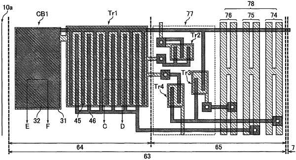
a shift register monolithically formed on the insulating substrate, the shift register being arranged in a region between the first end and the display region, wherein:
the shift register includes a plurality of unit circuits that are multistage-connected and a first wiring connected to the plurality of unit circuits,
the plurality of unit circuits include a first unit circuit and a second unit circuit,
the first unit circuit includes:
a clock terminal of the first unit circuit into which a clock signal is input,
an output terminal of the first unit circuit outputting an output signal,
a first transistor including a source electrode and a drain electrode, one of the source electrode and the drain electrode being connected to the clock terminal of the first unit circuit and another of the source electrode and the drain electrode being connected to the output terminal of the first unit circuit,
a second transistor connected to the first transistor and an output terminal of the second unit circuit, and
a first capacitor including a first terminal connected to a gate electrode of the first transistor and a second terminal connected to the output terminal of the first unit circuit,
the first wiring connected to the plurality of unit circuits supplies a first potential to turn off the pixel transistor or the first transistor to the plurality of unit circuits,
the first transistor and the first capacitor are arranged in a region between the first end and the first wiring,
the second transistor is arranged in a region between a part of the first capacitor and the first wiring.
|