| CPC G02F 1/1339 (2013.01) [G02F 1/133345 (2013.01); G02F 1/133388 (2021.01)] | 11 Claims |
|
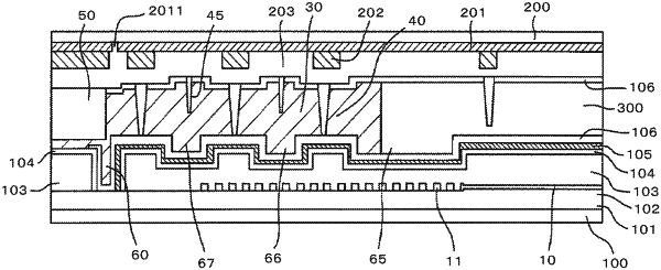
1. A display device comprising:
a first substrate having a first inorganic film, an organic film provided on the first inorganic film, a plurality of lines provided between the first inorganic film and the organic film, a second inorganic film provided on the organic film, and a transparent conductive film provided on the second inorganic film;
a second substrate opposed to the first substrate; and
a sealing material bonded the first substrate and the second substrate,
wherein
the sealing material is located in a peripheral area which surrounds a display area,
the plurality of lines is located in the peripheral area, and overlapped with the sealing material in a plan view,
the organic film has a hole in the peripheral area,
the transparent conductive film is located between the hole and the display area, and overlapped with the plurality of lines and the sealing material in the plan view,
the plurality of lines does not overlap the hole in the plan view,
the transparent conductive film and the plurality of lines are not connected to each other,
the second inorganic film contacts to the first inorganic film in the hole, and
the transparent conductive film is in contact with the first inorganic film in the hole.
|