| CPC G02F 1/133308 (2013.01) [G02F 1/13338 (2013.01); G02F 1/133528 (2013.01); B32B 7/12 (2013.01); G02F 1/133331 (2021.01); G02F 2202/28 (2013.01)] | 7 Claims |
|
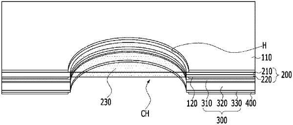
1. A method of manufacturing a display device comprising:
preparing a display panel and a polarization plate on the display panel, the display panel having a transparent portion and the polarization plate having a through hole corresponding to the transparent portion of the display panel;
disposing an optical clear resin (OCR) layer in the through hole of the polarization plate, the OCR layer overlapping the transparent portion of the display panel without overlapping a non-transparent portion of the display panel;
attaching an optically clear adhesive (OCA) film to a cover substrate; and
combining the polarization plate with the OCA film attached to the cover substrate.
|