| CPC G02B 6/4215 (2013.01) [G02B 6/2813 (2013.01); G02B 6/29349 (2013.01); G02B 6/4287 (2013.01)] | 10 Claims |

|
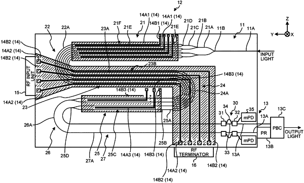
1. An optical device comprising:
a modulator that includes
an optical waveguide that is formed of a thin-film lithium niobate (LN) substrate and through which light passes; and
an electrode that applies voltage to the optical waveguide, and
modulates a phase of the light that passes through the optical waveguide in accordance with an electric field in the optical waveguide, the electric field corresponding to the voltage;
a tap coupler that includes at least a part formed of the thin-film LN substrate, and splits a part of the light that passes through an inside of the optical waveguide; and
a monitor that is coupled to the tap coupler and monitors the part of the light split by the tap coupler;
wherein
the tap coupler includes a delayed interferometer that splits a part of the light that passes through the optical waveguide, at a split ratio corresponding to a phase difference of light that passes through an inside of the tap coupler from the optical waveguide; and
wherein the delayed interferometer includes
a first coupler that receives the light input from the optical waveguide and splits the input light;
a first waveguide that is formed of the thin-film LN substrate and through which one part of light split from the first coupler passes;
a second waveguide that is formed of the thin-film LN substrate, through which other part of light split from the first coupler passes, and that delays optical output as compared to the first waveguide; and
a second coupler that multiplexes the one part of light from the first waveguide and the other part of light from the second waveguide, and splits the multiplexed light with a phase difference at a split ratio corresponding to the phase difference.
|