| CPC G02B 6/12007 (2013.01) [G02B 6/14 (2013.01); G02B 2006/12152 (2013.01); G02B 2006/12164 (2013.01)] | 3 Claims |
|
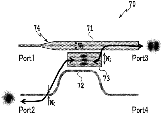
1. A mode multiplexing/demultiplexing optical circuit including a first waveguide and a second waveguide formed on a planar light wave circuit, the mode multiplexing/demultiplexing optical circuit comprising:
a first input/output port configured to allow light from a light source to be input to the first waveguide;
a second input/output port configured to allow the light propagating through the first waveguide to be output;
a mode conversion unit located adjacent to the first waveguide, and configured to convert a mode of light input from the second input/output port to a mode of a higher order than an order of the mode when the light is input to the second input/output port; and
a third output port configured to convert, via the second waveguide located adjacent to the mode conversion unit, a mode of light input to the mode conversion unit to a mode of a lower order than the order of the mode when the light is input to the second input/output port, and output the converted light,
wherein the first waveguide, the mode conversion unit, and the second waveguide are adjacent to each other in this order, and widths of the waveguides at adjacent locations satisfy a relationship: a width of the mode conversion unit>a width of the first waveguide>a width of the second waveguide.
|