| CPC G01T 1/1644 (2013.01) [A61B 6/037 (2013.01); G01T 1/208 (2013.01)] | 7 Claims |
|
1. A PET detector for reducing the number of silicon photomultiplier tubes in use, wherein:
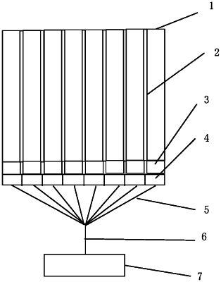
the detector comprises a layer formed by scintillation crystal array units and a layer formed by silicon photomultiplier tube array units respectively, the scintillation crystal array units and the silicon photomultiplier tube array units each have a rectangular cross section in the top view, and the top-view rectangular cross sections of the scintillation crystal array units and the silicon photomultiplier tube array units have the same area;
the scintillation crystal array unit is composed of a plurality of mutually parallel scintillation crystal strips, the scintillation crystal strips are each rectangular parallelepipeds having the same specifications in terms of each of the length, the width and the height, and each two of the scintillation crystal strips are provided with a reflective material therebetween or surfaces of the scintillation crystal strips are plated with a reflective material;
the silicon photomultiplier tube array unit is an array aggregate with a rectangular cross section in the top view formed by arranging M silicon photomultiplier tube arrays;
N blocks in the silicon photomultiplier tube array unit are replaced with high-reflectivity material blocks, and the high-reflectivity material block is integrally formed by using a mold adapted to the shape of the silicon photomultiplier tube array unit, or is formed by cutting; the high-reflectivity material block is made entirely of a uniform high-reflectivity material, or a side of the high-reflectivity material block that faces the scintillation crystal array unit is coated with a high-reflectivity material, and the reflectivity of the side of the high-reflectivity material block that faces the scintillation crystal array unit is not less than 50%; and
both M and N are natural numbers greater than 1, and M−N≥1.
|