| CPC G01R 31/2836 (2013.01) [H05K 1/0268 (2013.01); H05K 3/00 (2013.01)] | 18 Claims |
|
1. A method for locating an open circuit failure point of a test structure, comprising:
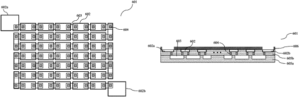
step 1: providing a sample formed with the test structure,
the test structure comprising a lower layer structure, an intermediate layer, and an upper layer structure, the lower layer structure comprising a plurality of first metal layer patterns, the intermediate layer comprising a plurality of vias, the upper layer structure comprising a plurality of second metal layer patterns, each first metal layer pattern and each second metal layer pattern forming a series resistor structure through each via, and the second metal layer patterns at two ends of the series resistor structure forming a first test end and a second test end,
the first metal layer patterns of the lower layer structure being isolated by a lower layer interlayer film,
the second metal layer patterns of the upper layer structure and the vias of the intermediate layer being isolated by an upper layer interlayer film,
the upper layer structure further comprising a metal diffusion blocking layer, the metal diffusion blocking layer covering surfaces of the second metal layer patterns and the upper interlayer film, and
removing the metal diffusion blocking layer on tops of the first test end and the second test end in the test structure of the sample to expose the first test end and the second test end;
step 2: performing a first active voltage contrast test to the sample to show an open circuit point of the test structure, making a first scratch mark at an adjacent position of the open circuit point, and then ending the first active voltage contrast test;
step 3: finding the first scratch mark on the sample and forming a coating mark at the first scratch mark; and
step 4: performing a second active voltage contrast test to the sample to show the open circuit point and locating a relative position of the open circuit point by using a position of the coating mark as a reference position according to a feature that the coating mark is adjacent to the open circuit point.
|