| CPC G01J 1/44 (2013.01) [G01J 1/0252 (2013.01); G06F 21/71 (2013.01); G06F 21/87 (2013.01); G01J 2001/446 (2013.01); H01L 23/576 (2013.01)] | 20 Claims |
|
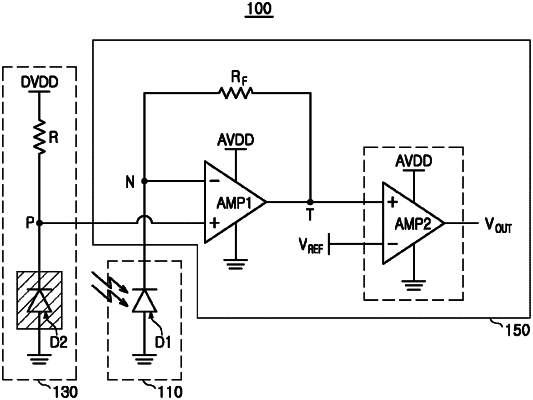
1. A semiconductor device comprising:
a sensing circuit including a first semiconductor element configured to generate a first current in response to externally incident light;
a compensation circuit including a second semiconductor element configured to generate a second current depending on an ambient temperature, wherein the compensation circuit is configured to remove the second current from the first current to generate a third current;
a detection circuit configured to convert the third current into a photovoltage and to compare the photovoltage with a predetermined reference voltage to determine whether an external attack has occurred; and
a defense circuit configured to control the semiconductor device to perform a predetermined defense operation, based on a result of the determination.
|