| CPC C23C 14/35 (2013.01) [C23C 14/0036 (2013.01); C23C 14/046 (2013.01); C23C 14/0641 (2013.01); C23C 14/225 (2013.01); C23C 14/3492 (2013.01); C23C 14/358 (2013.01); C23C 16/045 (2013.01); C23C 16/34 (2013.01); C23C 16/45525 (2013.01); H01J 37/3405 (2013.01); H01J 37/3458 (2013.01); H01L 21/02183 (2013.01); H01L 21/02266 (2013.01); H01L 21/2855 (2013.01); H01L 21/67253 (2013.01); H01L 21/76831 (2013.01); H01L 21/76843 (2013.01); H01L 21/28568 (2013.01); H01L 21/32051 (2013.01); H01L 23/53238 (2013.01)] | 20 Claims |
|
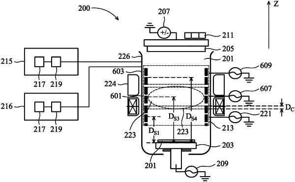
1. A deposition system comprising:
a first deposition chamber;
a target within the first deposition chamber;
a mounting platform within the first deposition chamber;
a first coil within the first deposition chamber;
a first power source connected to the first coil;
a second coil within the first deposition chamber;
a second power source connected to the second coil;
a third coil within the first deposition chamber;
a third power source connected to the third coil, wherein the first power source, the second power source and the third power source are each different; and
a second deposition chamber, the second deposition chamber connected to a second precursor delivery system, the second deposition chamber being an atomic layer deposition chamber.
|