| CPC B81C 1/00238 (2013.01) [H01L 21/02274 (2013.01); H01L 21/31053 (2013.01); H01L 22/12 (2013.01)] | 20 Claims |
|
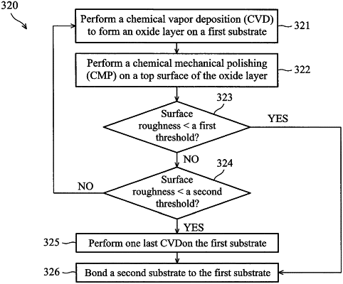
1. A method for bonding a pair of semiconductor substrates, wherein the pair of semiconductor substrates comprises a first semiconductor substrate and a second semiconductor substrate, the method comprising:
processing the first semiconductor substrate before bonding, wherein the processing before bonding comprises:
predetermining a first target surface roughness value and a second target surface roughness value, wherein the second target surface roughness value is from 200% to 300% of the first target surface roughness value,
repeating a cycle of performing chemical vapor deposition (CVD) of a dielectric material to form a dielectric layer on a top surface of the first semiconductor substrate followed by chemical mechanical polishing (CMP) on the top surface of the first semiconductor substrate when a roughness of the top surface is larger than or equal to the second target surface roughness value,
performing an additional CVD of the dielectric material on the top surface of the dielectric layer when the roughness of the top surface is smaller than the second target surface roughness value and larger than or equal to the first target surface roughness value; and
bonding the pair of semiconductor substrates together when the roughness of the top surface is smaller than the first target surface roughness value, wherein the second semiconductor substrate is in direct contact with the top surface of the dielectric layer.
|