| CPC B81B 3/0075 (2013.01) [B81C 1/00674 (2013.01); C23C 14/18 (2013.01); C23C 14/5806 (2013.01); C25D 3/562 (2013.01); C25D 5/50 (2013.01); B81B 2203/0118 (2013.01); B81C 2201/0132 (2013.01); B81C 2201/0133 (2013.01); B81C 2201/0181 (2013.01); B81C 2201/0197 (2013.01)] | 16 Claims |
|
1. A film comprising:
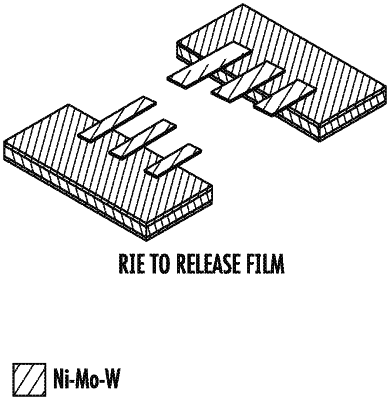
an alloy of nickel (Ni), molybdenum (Mo), tungsten (W) (Ni—Mo—W) having very high predetermined tensile strength, thermal and mechanical stability of predetermined levels, predetermined high density, predetermined low CTE, predetermined electrical properties that are similar to the bulk alloy, and a structure of nano-scale stacking faults and twins lying in a plane of the film;
wherein the alloy is deposited as a coating or freestanding thin film or device; and,
wherein the alloy comprises a crystallographic structure possessing a predetermined strong <111> crystallographic texture and a predetermined high density of nano-scale planar defects (stacking faults and twins) oriented in the plane of the film.
|