| CPC B81B 3/0005 (2013.01) [B81B 3/001 (2013.01); B81C 1/00968 (2013.01); B81B 2203/0127 (2013.01); B81B 2203/0315 (2013.01); B81B 2203/0392 (2013.01); B81B 2203/04 (2013.01); B81C 2201/112 (2013.01); B81C 2203/036 (2013.01)] | 20 Claims |
|
1. A microelectromechanical system (MEMS) device comprising:
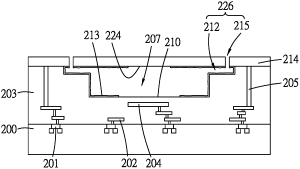
a substrate;
a dielectric layer being formed on the substrate, and being formed with a cavity that is defined by a cavity-defining wall;
an electrode formed in the dielectric layer;
a surface modification layer covering the cavity-defining wall, the surface modification layer having a plurality of hydrophobic end groups;
a membrane connected to the dielectric layer and sealing the cavity, the membrane being movable toward or away from the electrode;
a venting passage penetrating the membrane and the dielectric layer and being in spatial communication with the cavity; and
a seal sealing the venting passage so as to hermetically isolate the cavity from the outside environment.
|