| CPC B23K 3/0623 (2013.01) [B23K 3/082 (2013.01); H01L 24/11 (2013.01); H01L 24/75 (2013.01); H05K 3/34 (2013.01)] | 2 Claims |
|
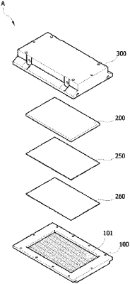
1. A flux tool of flux printing equipment for dotting flux for attaching solder balls to a wafer of a semiconductor chip package, the flux tool comprising:
a pin block having a plurality of pin holes formed thereon in a pattern and a plurality of flux pins configured to be inserted into the pin holes; and
at least one elastic pad disposed on top of the pin block to pressurize the flux pins,
wherein the number of the flux pins corresponds to the number of the pin holes, such that, in dipping and dotting processes, the flux pins inserted into the pin holes move upward and downward from the pin holes, independently of one another, and the elastic pad has a conductive film located on an underside thereof,
wherein the conductive film is made of a non-metal conductive material, and the elastic pad includes an additional film located on an underside of the conductive film, the additional film having a hardness greater than those of the conductive film and the elastic pad.
|