| CPC G06F 15/7825 (2013.01) [G06F 13/42 (2013.01)] | 20 Claims |
|
1. A method comprising:
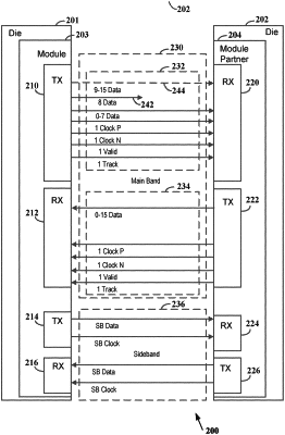
sending an enable request from a module of a first die to a module partner of a second die through a sideband to operate a main band of a die-to-die connection that connects the first die module to the second die module partner at a specified transmit link width, wherein the specified transmit link width has a specified set of transmit data lines of the main band;
receiving an enable response from the module partner through the sideband to operate the main band at the specified transmit link width;
sending a second enable request including from the module of the first die to the module partner of the second die through the sideband to operate the main band of the die-to-die connection that connects the first die module to the second die module partner at a specified receive link width, wherein the specified receive link width has a specified set of receive data lines of the main band;
receiving a second enable response from the module partner through the sideband to operate the main band at the specified receive link width; and
communicating data with the module partner through the main band using a specified link width in response to receiving the enable response, wherein the specified link width includes the specified transmit link width and the specified receive link width.
|