| CPC H03H 9/19 (2013.01) [B81B 3/0018 (2013.01); H01Q 1/12 (2013.01); H01Q 9/04 (2013.01); H10N 30/853 (2023.02); H03H 2009/155 (2013.01); Y10T 29/49016 (2015.01)] | 7 Claims |

|
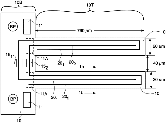
1. A method of making a RF antenna in which a magnetostrictive film is deposited on a quartz wafer, the method comprising:
patterning selected portions of a top surface of the quartz wafer for deposition of electrode metal and deposition of said magnetostrictive film and depositing said electrode metal and said magnetostrictive film;
temporarily bonding the quartz wafer to a handle wafer;
thinning the quartz wafer to a desired thickness;
etching the quartz wafer to define the outlines of at least one quartz resonator bearing said electrode metal and said magnetostrictive film;
patterning selected portions of a bottom surface the at least one quartz resonator for deposition of electrode metal and at least one bond pad and depositing said electrode metal and said at least one bond pad;
bonding the at least one quartz resonator to a substrate wafer; and
releasing the at least one quartz resonator from said handle wafer.
|