| CPC H10K 59/1315 (2023.02) [C22C 21/00 (2013.01); H10K 59/126 (2023.02); H10K 59/1213 (2023.02); H10K 59/1216 (2023.02); H10K 77/111 (2023.02); H01L 27/124 (2013.01); H01L 27/127 (2013.01); H01L 27/1222 (2013.01); H01L 27/1255 (2013.01); H01L 29/66757 (2013.01); H01L 29/78675 (2013.01); H10K 59/1201 (2023.02); H10K 2102/311 (2023.02)] | 17 Claims |

|
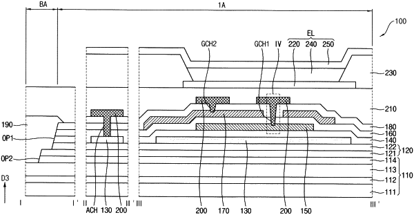
1. A display device comprising:
a base substrate;
a buffer layer disposed on the base substrate;
an active layer disposed on the buffer layer;
a first gate insulation layer disposed on the active layer;
a first conductive layer disposed on the first gate insulation layer and which is a single-layer including an aluminum alloy;
a second gate insulation layer disposed on the first conductive layer;
a second conductive layer disposed on the second gate insulation layer and which is a single-layer including an aluminum alloy;
an insulation interlayer disposed on the second conductive layer; and
a third conductive layer disposed on the insulation interlayer, directly contacting the first conductive layer through a first gate contact hole defined in the insulation interlayer and the second gate insulation layer, and directly contacting the second conductive layer through a second gate contact hole defined in the insulation interlayer,
wherein a thickness of a first portion of the first conductive layer which directly contacts the third conductive layer is less than a thickness of a second portion of the first conductive layer which does not directly contact the third conductive layer.
|