| CPC H10K 59/122 (2023.02) [H10K 50/844 (2023.02); H10K 59/353 (2023.02); H10K 59/40 (2023.02); H10K 71/00 (2023.02); H10K 59/1201 (2023.02)] | 15 Claims |

|
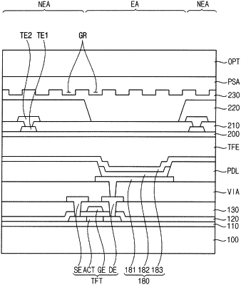
1. A display device comprising:
a base substrate;
a pixel defining layer disposed on the base substrate and including a first opening;
a light emitting structure disposed in the first opening of the pixel defining layer;
a thin film encapsulation layer disposed on the light emitting structure;
a touch electrode disposed on the thin film encapsulation layer;
an insulating pattern disposed on the touch electrode and including a second opening which overlaps the first opening; and
a high refractive layer disposed on the insulating pattern, the high refractive layer including:
a plurality of grid patterns disposed on a top surface of the high refractive layer, wherein the grid pattern is arranged such as to reduce deviation in white angular difference (WAD) in the display device; and
a refractive index higher than a refractive index of the insulating pattern.
|