| CPC H10K 59/1213 (2023.02) [H10K 59/126 (2023.02); H10K 59/1216 (2023.02); H10K 71/00 (2023.02); H01L 27/1225 (2013.01); H01L 27/1237 (2013.01); H01L 27/1251 (2013.01); H01L 27/1255 (2013.01); H01L 27/1288 (2013.01); H01L 29/42384 (2013.01); H01L 29/4908 (2013.01); H01L 29/66757 (2013.01); H01L 29/66969 (2013.01); H01L 29/7869 (2013.01); H01L 29/78633 (2013.01); H01L 29/78675 (2013.01); H10K 59/1201 (2023.02)] | 4 Claims |

|
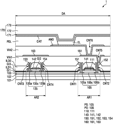
1. A method of manufacturing a display device comprising:
forming a first semiconductor pattern on a substrate;
forming a first gate insulating film covering the first semiconductor pattern;
forming a first conductive layer on the first gate insulating film;
forming a material layer for a second semiconductor layer on the first gate insulating film;
forming a material layer for a second gate insulating film on the material layer for the second semiconductor layer;
sequentially etching the material layer for the second gate insulating film and the material layer for the second semiconductor layer using a same etching mask and forming a second semiconductor pattern and the second gate insulating film on the second semiconductor pattern;
forming a third gate insulating film covering the second gate insulating film; and
forming a second conductive layer on the third gate insulating film,
wherein the first semiconductor pattern comprises a semiconductor layer of a first transistor,
wherein the second semiconductor pattern comprises a semiconductor layer of a second transistor, and a side surface of the second semiconductor pattern is aligned with a side surface of the second gate insulating film,
wherein the first conductive layer comprises a gate electrode of the first transistor and a first electrode of a capacitor, and
wherein the second conductive layer comprises a gate electrode of the second transistor and a second electrode of the capacitor,
wherein the third gate insulating film is between the first and second electrodes of the capacitor.
|