| CPC H10K 50/858 (2023.02) [G02B 3/00 (2013.01); G02B 3/0056 (2013.01); G02B 27/0955 (2013.01); G06F 3/03545 (2013.01); G06F 3/042 (2013.01); G06F 3/0412 (2013.01); G06F 3/0421 (2013.01); G06F 3/147 (2013.01); G09F 9/30 (2013.01); G09G 3/30 (2013.01); G09G 3/3225 (2013.01); H05B 33/02 (2013.01); H10K 50/00 (2023.02); H10K 59/00 (2023.02); H10K 59/12 (2023.02); H10K 59/60 (2023.02); G06F 3/16 (2013.01)] | 18 Claims |

|
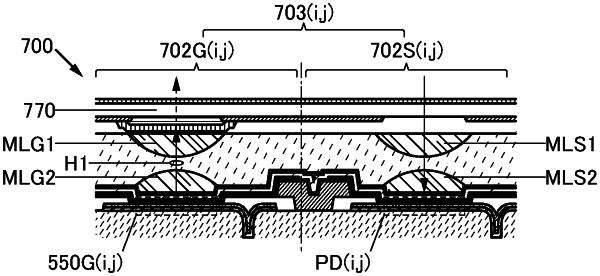
1. A functional panel comprising:
a base material; and
a pair of pixels,
wherein the base material covers the pair of pixels,
wherein the base material has a light-transmitting property,
wherein the pair of pixels comprises one pixel and another pixel,
wherein the one pixel comprises a light-emitting device and a first microlens,
wherein the light-emitting device emits light toward the base material,
wherein the first microlens is interposed between the base material and the light-emitting device,
wherein the first microlens converges light,
wherein the first microlens comprises a first surface and a second surface,
wherein the second surface is closer to the light-emitting device than the first surface is,
wherein the second surface has a smaller radius of curvature than the first surface,
wherein the second surface faces the light-emitting device,
wherein the other pixel comprises a photoelectric conversion device and a second microlens,
wherein the second microlens is interposed between the base material and the photoelectric conversion device,
wherein the second microlens converges external light incident from the base material side,
wherein the second microlens comprises a third surface and a fourth surface,
wherein the third surface faces the photoelectric conversion device,
wherein the third surface is closer to the photoelectric conversion device than the fourth surface is, and
wherein the fourth surface has a smaller radius of curvature than the third surface.
|