| CPC H10K 50/844 (2023.02) [H10K 59/122 (2023.02); H10K 59/124 (2023.02)] | 20 Claims |

|
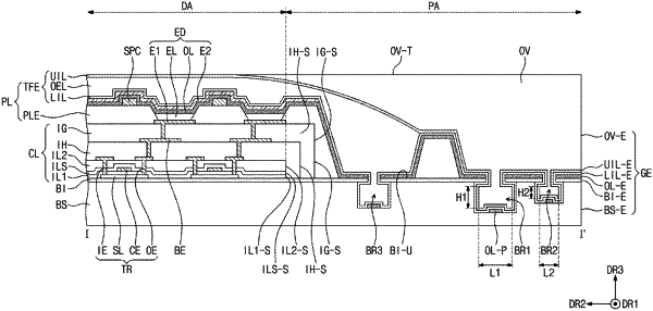
1. A display panel including a hole, a display region and a hole peripheral region between the hole and the display region, comprising:
a base substrate including a first groove and a second groove both in the hole peripheral region, the second groove is between the hole and the first groove;
a barrier layer on the base substrate;
a transistor on the barrier layer;
a first electrode coupled to the transistor;
a light emitting layer on the first electrode;
a second electrode on the light emitting layer;
a first inorganic encapsulation layer on the second electrode;
an organic encapsulation layer on the first inorganic encapsulation layer;
a second inorganic encapsulation layer on the organic encapsulation layer; and
an first organic layer on the second inorganic encapsulation layer;
wherein the first inorganic encapsulation layer and the second inorganic encapsulation layer are in the second groove,
wherein the first inorganic encapsulation layer is in the first groove,
wherein the first organic layer is in the second groove.
|