| CPC H10B 41/41 (2023.02) [H01L 29/40114 (2019.08); H01L 29/40117 (2019.08); H01L 29/42328 (2013.01); H01L 29/42344 (2013.01); H10B 41/10 (2023.02); H10B 41/35 (2023.02); H10B 43/10 (2023.02); H10B 43/35 (2023.02); H10B 43/40 (2023.02); H01L 29/66825 (2013.01); H01L 29/66833 (2013.01); H01L 29/7889 (2013.01); H01L 29/7926 (2013.01)] | 19 Claims |

|
1. A semiconductor device, comprising:
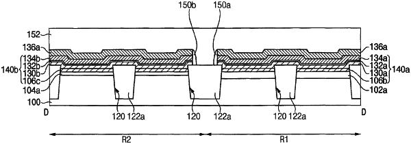
a substrate that includes a first active region, a second active region, and an isolation region in a trench between the first and second active regions;
an isolation layer pattern that fills the trench;
a first gate insulation layer pattern disposed on the substrate;
a first gate electrode structure disposed on the first gate insulation layer pattern, wherein the first gate electrode structure extends in a first direction and crosses the first active region, and wherein the first gate electrode structure includes a first polysilicon pattern, a second polysilicon pattern, and a first metal pattern that are sequentially stacked;
a second gate insulation layer pattern disposed on the substrate; and
a second gate electrode structure disposed on the second gate insulation layer pattern, wherein the second gate electrode structure extends in the first direction and crosses the second active region, and wherein the second gate electrode structure including a third polysilicon pattern, a fourth polysilicon pattern, and a second metal pattern thin are sequentially stacked,
wherein an upper surface of the isolation layer pattern is higher than an upper surface of each of the first and third polysilicon patterns, and a sidewall of each of the first and third polysilicon patterns contacts a sidewall of the isolation layer pattern,
wherein the first gate insulation layer pattern and the second gate insulation layer pattern have different thicknesses, and
wherein upper surfaces of the first gate insulation layer pattern and the second gate insulation layer pattern are substantially coplanar with each other.
|