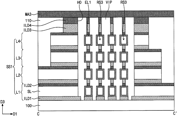
| CPC H10B 41/27 (2023.02) [G11C 7/18 (2013.01); G11C 8/14 (2013.01); H01L 23/53295 (2013.01); H01L 28/60 (2013.01); H10B 41/35 (2023.02); G11C 11/404 (2013.01); G11C 11/4097 (2013.01)] | 20 Claims |

|
1. A method for manufacturing a semiconductor memory device, the method comprising:
forming a plurality of semiconductor layers stacked on a substrate;
forming a vertical insulation pattern extending through one or more of the plurality of semiconductor layers and defining one or more semiconductor patterns from the plurality of semiconductor layers;
forming one or more recessions by selectively etching the one or more semiconductor patterns, respectively;
expanding the one or more recessions by partially etching the vertical insulation pattern;
forming at least one first electrode in the one or more recessions, respectively;
forming a dielectric layer on the at least one first electrode; and
forming a second electrode on the dielectric layer.
|