| CPC H10B 41/27 (2023.02) [H01L 23/5384 (2013.01); H01L 25/0657 (2013.01); H10B 43/27 (2023.02)] | 20 Claims |

|
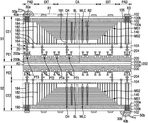
1. A semiconductor memory device comprising:
a first semiconductor chip including an upper input/output pad;
a second semiconductor chip including a lower input/output pad; and
a substrate attachment film which attaches the first semiconductor chip and the second semiconductor chip,
wherein each of the first semiconductor chip and the second semiconductor chip further includes:
a first substrate which includes a first side facing the substrate attachment film and a second side opposite to the first side,
a mold structure including a plurality of gate electrodes stacked sequentially on the first side of the first substrate,
a channel structure which penetrates the mold structure and intersects the plurality of gate electrodes,
a second substrate which includes a third side facing the first side and a fourth side opposite to the third side,
a first circuit element on the third side of the second substrate, and
a contact via which penetrates the first substrate and is connected to the first circuit element,
wherein the substrate attachment film attaches the second substrate of the first semiconductor chip and the second substrate of the second semiconductor chip,
wherein the upper input/output pad is placed on the second side of the first semiconductor chip and contacts the contact via of the first semiconductor chip, and
wherein the lower input/output pad is placed on the second side of the second semiconductor chip and contacts the contact via of the second semiconductor chip.
|