| CPC H10B 12/315 (2023.02) [H10B 12/0335 (2023.02); H10B 12/37 (2023.02); H10B 12/482 (2023.02)] | 7 Claims |

|
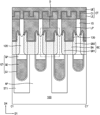
1. A semiconductor device, comprising:
an active pattern;
a gate structure connected to the active pattern;
a bit line structure connected to the active pattern;
a buried contact connected to the active pattern;
a contact pattern covering the buried contact;
a landing pad connected to the contact pattern; and
a capacitor structure connected to the landing pad,
wherein:
the buried contact includes a first growth portion and a second growth portion spaced apart from each other, and
the landing pad includes an interposition portion between the first growth portion and the second growth portion.
|