| CPC H05K 1/111 (2013.01) [H05K 2201/09409 (2013.01)] | 20 Claims |

|
1. A printed circuit board, comprising:
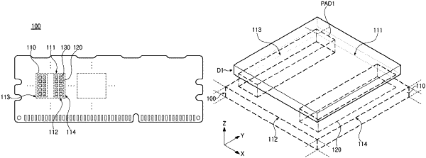
a base substrate having a first side and a second side, extending in a first direction and parallel to each other, and a third side and a fourth side extending in a second direction, perpendicular to the first direction, and parallel to each other;
a pad region having a plurality of pad patterns disposed on one surface of the base substrate; and
a dummy region having a plurality of conductive dummy patterns separated from the plurality of pad patterns to be disposed on the one surface of the base substrate, wherein:
the pad region includes a first edge region adjacent to an intersection of the first side and the third side, and a second edge region disposed in a diagonal direction of the first edge region on the one surface of the base substrate, and
the dummy region includes a third edge region adjacent to an intersection of the first side and the fourth side, and a fourth edge region disposed in a diagonal direction of the third edge region on the one surface of the base substrate.
|