| CPC H04N 25/772 (2023.01) [H04N 25/75 (2023.01)] | 20 Claims |

|
1. An imaging device, comprising:
a plurality of pixels, each of which includes a light receiving element that generates an electric charge by photoelectric conversion in response to received light,
a pixel circuit that reads the electric charge from the light receiving element and outputs an analog signal corresponding to the electric charge, and
a conversion circuit that converts the analog signal into a digital signal on the basis of comparison results obtained by comparing the analog signal and a reference signal whose voltage changes stepwise at a constant slope over time;
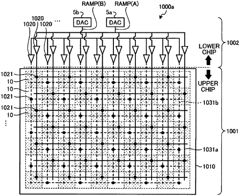
a generation unit that generates, as reference signals, a first reference signal to be supplied to a first pixel of the plurality of pixels and a second reference signal to be supplied to a second pixel of the plurality of pixels different from the first pixel;
a first wiring that connects the generation unit and the first pixel; and
a second wiring that connects the generation unit and the second pixel, wherein
the first reference signal is supplied to the first pixel via the first wiring, and
the second reference signal is supplied to the second pixel via the second wiring.
|