US 11,843,886 B2
Solid-state imaging device and manufacturing method therefor
Mineo Shimotsusa, Machida (JP); and Fumihiro Inui, Yokohama (JP)
Assigned to CANON KABUSHIKI KAISHA, Tokyo (JP)
Filed by CANON KABUSHIKI KAISHA, Tokyo (JP)
Filed on Aug. 3, 2021, as Appl. No. 17/393,078.
Application 17/393,078 is a continuation of application No. 16/579,058, filed on Sep. 23, 2019, granted, now 11,108,982.
Application 16/579,058 is a continuation of application No. 15/702,097, filed on Sep. 12, 2017, granted, now 10,462,405, issued on Oct. 29, 2019.
Application 15/702,097 is a continuation of application No. 15/239,530, filed on Aug. 17, 2016, granted, now 9,787,931, issued on Oct. 10, 2017.
Application 15/239,530 is a continuation of application No. 14/555,352, filed on Nov. 26, 2014, granted, now 9,450,012, issued on Sep. 20, 2016.
Application 14/555,352 is a continuation of application No. 13/807,065, granted, now 8,928,041, issued on Jan. 6, 2015, previously published as PCT/JP2011/003530, filed on Jun. 21, 2011.
Claims priority of application No. JP2010-149476 (JP), filed on Jun. 30, 2010.
Prior Publication US 2021/0368120 A1, Nov. 25, 2021
Int. Cl. H01L 27/146 (2006.01); H04N 25/75 (2023.01)
CPC H04N 25/75 (2023.01) [H01L 27/1463 (2013.01); H01L 27/1464 (2013.01); H01L 27/14601 (2013.01); H01L 27/14609 (2013.01); H01L 27/14612 (2013.01); H01L 27/14621 (2013.01); H01L 27/14623 (2013.01); H01L 27/14627 (2013.01); H01L 27/14632 (2013.01); H01L 27/14634 (2013.01); H01L 27/14636 (2013.01); H01L 27/14641 (2013.01); H01L 27/14643 (2013.01); H01L 27/14683 (2013.01)] 20 Claims
OG exemplary drawing
 
1. A device comprising:
a first semiconductor substrate; and
a second semiconductor substrate overlapping the first semiconductor substrate,
wherein
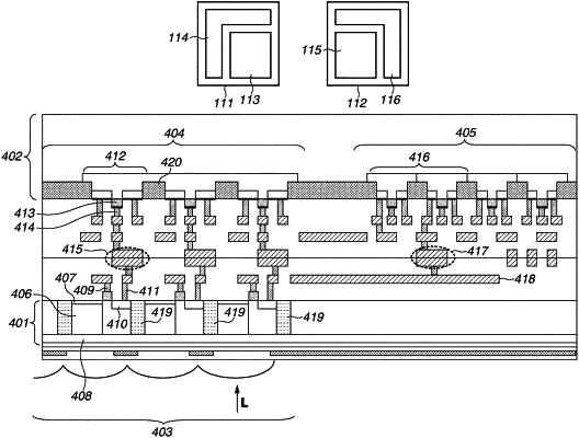
the first semiconductor substrate includes a first pixel region where a plurality of photoelectric conversion units included in a plurality of pixels are arranged;
wherein the second semiconductor substrate includes a second pixel region including a part of a pixel included in the plurality of pixels and a first peripheral circuit region arranged around the second pixel region;
wherein in plan view, the first pixel region overlaps the second pixel region, and
wherein in plan view, at least a part of the first peripheral circuit region does not overlap the first pixel region.