| CPC H04M 1/72466 (2021.01) [G06F 1/1626 (2013.01); G06F 1/1656 (2013.01); G06F 1/1684 (2013.01); G06F 1/1694 (2013.01); G06F 3/041 (2013.01); G06F 3/0421 (2013.01); G06F 3/0488 (2013.01); G06F 3/04886 (2013.01); G06F 2200/1614 (2013.01); G06F 2200/1637 (2013.01); H04M 2250/12 (2013.01); H04M 2250/22 (2013.01)] | 14 Claims |

|
1. A mobile information-communication device comprising:
a display element;
a sensor part electrically connected to the display element;
an arithmetic circuit electrically connected to the display element; and
a gradient detection portion electrically connected to the arithmetic circuit,
wherein the sensor part comprises:
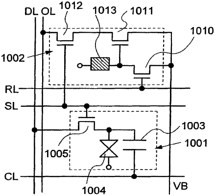
a first transistor;
a second transistor;
a third transistor; and
a photodiode,
wherein one of a source and a drain of the first transistor is electrically connected to an output wiring,
wherein the other of the source and the drain of the first transistor is electrically connected to one of a source and a drain of the second transistor,
wherein a gate of the second transistor is electrically connected to one of a source and a drain of the third transistor through a first conductive layer,
wherein the first conductive layer is electrically connected to a first electrode of the photodiode,
wherein the other of the source and the drain of the second transistor is electrically connected to a power supply line,
wherein the other of the source and the drain of the third transistor is electrically connected to the power supply line,
wherein a second electrode of the photodiode is electrically connected to a first wiring extending in a first direction,
wherein the first wiring is electrically connected to a second wiring extending in a second direction being perpendicular to the first direction,
wherein the first conductive layer, the first wiring, and the power supply line are provided in a first layer,
wherein a gate of the first transistor is electrically connected to a first scan line,
wherein a gate of the third transistor is electrically connected to a second scan line,
wherein the second wiring, the first scan line, and the second scan line are provided in a second layer, and
wherein the gradient detection portion is configured to detect gradient of the mobile information-communication device and output signals in accordance with the gradient of the mobile information-communication device to the arithmetic circuit.
|