| CPC H04B 1/04 (2013.01) [H03F 3/245 (2013.01); H03F 2200/294 (2013.01); H03F 2200/451 (2013.01); H04B 2001/0408 (2013.01)] | 20 Claims |

|
1. An electronic device comprising:
a first antenna;
a first power amplifier (PA);
a first low noise amplifier (LNA);
a switch electrically connected to the first antenna, the first antenna being selectively connected to the first PA or the first LNA through the switch;
a bias control circuit configured to control a supply of a bias current driving the first PA; and
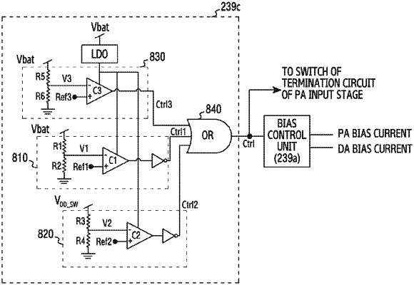
a voltage protection circuit electrically connected to the bias control circuit,
wherein the voltage protection circuit is configured to:
compare a first voltage provided by a battery with a first reference voltage and a second reference voltage respectively, the first reference voltage being higher than the second reference voltage, and
control the bias control circuit to supply the first PA with the bias current based on a result of comparing the first voltage with the first reference voltage and the second reference voltage.
|