| CPC H03K 19/018521 (2013.01) [H03K 19/00361 (2013.01)] | 9 Claims |

|
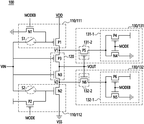
8. A buffer circuit comprising:
a power control circuit configured to provide a first power supply voltage and a second power supply voltage as a first voltage and a second voltage according to an input signal in a first operation mode and configured to provide the first power supply voltage and the second power supply voltage as the first voltage and the second voltage, regardless of the input signal, in a second operation mode;
an inverting circuit configured to receive the first voltage and the second voltage and configured to invert the input signal to generate an output signal; and
a voltage adjustment circuit configured to:
provide the second power supply voltage as the first voltage and provide the first power supply voltage as the second voltage based on the output signal in the first operation mode, and
provide the first power supply voltage as the first voltage and provide the second power supply voltage as the second voltage based on the output signal in the second operation mode.
|