| CPC H02M 7/4815 (2021.05) [H02M 1/0003 (2021.05); H02M 1/0025 (2021.05); H02M 1/4241 (2013.01); H02M 3/01 (2021.05); H02M 3/33571 (2021.05); H02M 3/33573 (2021.05)] | 15 Claims |

|
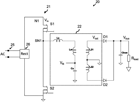
1. A resonant inverter, comprising:
an input node for receiving an input voltage for conversion;
a switch network, connected to the input node, comprising at least a first and second switches coupled in series, wherein a first switch output is defined from a node located between the first and second switches;
a resonant tank circuit coupled to the first switch output and adapted to output an alternating signal, wherein an electrical feedback parameter is provided by the resonant tank circuit;
a sampling circuit adapted to sample the electrical feedback parameter provided by the resonant tank circuit at a time of sampling;
a control circuit for generating a switch drive signal in dependence of the sampled electrical feedback parameter, the switch drive signal indicating a switching state for the first and second switches;
a switch driver adapted to control the switching state of the first and second switches responsive to a gate drive signal, wherein a change in the switching state of the first and second switches induces a change in the first switch output; and
a timing module adapted to monitor at least a voltage at the node of the resonant inverter to determine a time delay between a change in the switch drive signal and a corresponding change in the first switch output,
wherein the time of sampling is dependent upon the change in the switch drive signal and the sampling circuit is adapted to adjust the time of sampling and/or a value of the sampled electrical feedback parameter dependent upon the time delay.
|