| CPC H01M 50/483 (2021.01) [H01M 2200/00 (2013.01); H01M 2220/30 (2013.01)] | 19 Claims |

|
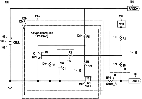
1. A battery for a portable communication device, the battery comprising:
a cell having positive and negative cell terminals;
positive and negative radio contact terminals operatively coupled to the positive and negative cell terminals to provide a common charge/discharge path to the battery;
a plurality of active current limit protection circuits coupled in series in the common charge/discharge path;
a pre-biasing circuit coupled to the plurality of series coupled active current limit protection circuits;
wherein the plurality of active current limit protection circuits each comprise:
a bipolar transistor switch;
biasing circuitry; and
a field effect transistor (FET) switch;
a current sense resistor coupled in series with the plurality of active current limit protection circuits, the current sense resistor and a FET from the plurality of active current limit protection circuits positioned in the common charge/discharge path, the current sense resistor and the FET providing a voltage drop across the current sense resistor and the FET, the voltage drop being indicative of a load current present on the battery; and
wherein the plurality of active current limit protection circuits comprises at least first and second active current limit protection circuits, the first current limit protection circuit being configured to:
turn ON a first bipolar transistor which turns OFF a first FET switch of the first active current limit protection circuit during an excessive current condition of the load current, thereby blocking current through the common charge/discharge path; and
turn OFF the first bipolar transistor which turns ON the first FET switch during recovery from the over current condition of the load current;
and
under conditions in which the first FET is damaged and does not turn OFF in response to the excessive current condition, the second current limit protection circuit being configured to:
turn ON a second bipolar transistor which turns OFF a second FET switch of the second active current limit protection circuit during the excessive current condition of the load current, thereby blocking current through the common charge/discharge path; and
turn OFF the second bipolar transistor which turns ON the second FET switch during recovery from the over current condition of the load current.
|