| CPC H01L 33/62 (2013.01) [H01L 33/06 (2013.01); H01L 33/10 (2013.01); H01L 33/14 (2013.01); H01L 33/32 (2013.01); H01L 33/36 (2013.01); H01L 33/38 (2013.01); H01L 33/382 (2013.01); H01L 33/385 (2013.01); H01L 33/387 (2013.01); H01L 33/40 (2013.01); H01L 33/405 (2013.01); H01L 33/42 (2013.01); H01L 33/44 (2013.01); H01L 33/46 (2013.01); H01L 33/60 (2013.01); H01L 2924/0002 (2013.01); H01L 2933/0016 (2013.01); H01L 2933/0025 (2013.01); H01L 2933/0066 (2013.01); H10K 50/814 (2023.02)] | 22 Claims |

|
1. A solid state lighting (“SSL”) device, comprising:
an SSL structure having a first semiconductor material, a second semiconductor material spaced apart from the first semiconductor material, and an active region between the first and second semiconductor materials;
a first contact on the first semiconductor material; and
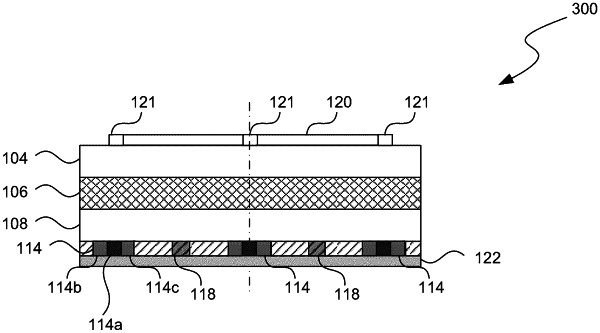
a second contact on the second semiconductor material, the second contact including a conductive material encapsulating a plurality of pads of a contact material, the plurality of pads of the contact material being sized to spatially modulate a current density of the SSL structure, the plurality of pads of the contact material each having an inner conductive portion with an inner portion contact resistance and an outer conductive portion surrounding the inner conductive portion, the outer conductive portion having an outer portion contact resistance greater than the inner portion contact resistance,
wherein the plurality of pads of the contact material form an interface with the second semiconductor material having a first contact resistance, and wherein the conductive material has a second contact resistance higher than the first contact resistance.
|