| CPC H01L 31/1868 (2013.01) [H01L 31/02366 (2013.01); H01L 31/03685 (2013.01); H01L 31/068 (2013.01); H01L 31/1824 (2013.01)] | 20 Claims |

|
1. A solar cell, comprising:
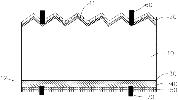
a semiconductor substrate, wherein a rear surface of the semiconductor substrate include a first texture structure, the first texture structure has a non-pyramid-shaped microstructure and includes two or more first substructures at least partially stacked on one another, a top surface of the first substructure is a polygonal plane, and a one-dimensional size of the top surface of the outermost first substructure is less than or equal to 45 μm; and wherein a front surface of the semiconductor substrate has a second texture structure, the second texture structure includes a pyramid-shaped microstructure, the pyramid-shaped microstructure includes a top portion away from the front surface of the semiconductor substrate and a bottom portion close to the front surface of the semiconductor substrate, and in a direction away from the front surface and perpendicular to the front surface, a distance between the top portion and the bottom portion of the pyramid-shaped microstructure is less than or equal to 5 μm;
a first passivation layer located on the second texture structure of the front surface of the semiconductor substrate;
a tunnel oxide layer located on the first texture structure of the rear surface of the semiconductor substrate;
a doped conductive layer located on a surface of the tunnel oxide layer, wherein the doped conductive layer includes a P-type doped conductive layer and an N-type doped conductive layer; and
a second passivation layer located on a surface of the doped conductive layer.
|