| CPC H01L 31/022433 (2013.01) [H01L 31/0201 (2013.01); H01L 31/022425 (2013.01); H01L 31/022441 (2013.01); H01L 31/0352 (2013.01); H01L 31/048 (2013.01); H01L 31/0504 (2013.01); H01L 31/0508 (2013.01); H01L 31/06 (2013.01); H10K 30/87 (2023.02); Y02E 10/50 (2013.01)] | 16 Claims |

|
1. A solar cell panel, comprising:
a plurality of solar cells; and
a plurality of wires that electrically interconnect adjacent solar cells among the plurality of solar cells, with each of the plurality of wires having a rounded cross-section,
wherein each of the plurality of solar cells comprises:
a semiconductor substrate that is rectangular-shaped having at least one long side and at least one short side,
a first electrode, and
a second electrode,
wherein the first electrode comprises:
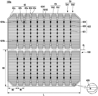
a plurality of finger electrodes arranged lengthwise along a first direction parallel to the at least one long side of the semiconductor substrate, and
a plurality of bus electrodes comprising a plurality of contact pads that are arranged along a second direction parallel to the at least one short side of the semiconductor substrate, the second direction being different from the first direction,
wherein the plurality of wires extend lengthwise along the second direction and are soldered to the plurality of contact pads,
wherein the plurality of contact pads are spaced apart from one another in the second direction to thereby define a space between neighboring two contact pads among the plurality of contact pads,
wherein the at least one long side includes a first long side and a second long side that is spaced apart from the first long side in the second direction,
wherein the semiconductor substrate comprises an edge area that is located at an edge portion of the semiconductor substrate, at least one of the plurality of wires being located at the edge area,
wherein the edge area comprises:
a first edge area at which one of the plurality of wires is located, the first edge area being disposed adjacent to the first long side, and
a second edge area disposed adjacent to the second long side in the second direction,
wherein a density of the first electrode in each of the first and second edge areas is less than a density of the plurality of finger electrodes in another area of the semiconductor substrate,
wherein the plurality of contact pads comprise a first outer pad that faces the first edge area, a second outer pad that faces the second edge area, and a plurality of inner pads disposed between the first outer pad and the second outer pad in the second direction,
wherein the first edge area separates the first outer pad from the edge portion of the semiconductor substrate in the second direction such that one of the plurality of wires is attached to the first electrode,
wherein at least one of the plurality of finger electrodes is arranged between two adjacent inner pads among the plurality of inner pads,
wherein a first length of the first or second outer pad in the second direction is greater than a second length of one of the plurality of inner pads in the second direction,
wherein the first electrode further comprises a peripheral portion that extends from an end of one of the bus electrodes or first outer pad to an end of an outermost finger electrode proximate the edge portion of the semiconductor substrate,
wherein the first electrode further comprises an edge electrode portion that is disposed at the first edge area or the second edge area, that is connected to one end of the plurality of wires, and that is connected to the plurality of finger electrodes, and
wherein the edge electrode portion comprises:
a first electrode portion that is disposed inward in the second direction relative to the outermost finger electrode among the plurality of finger electrodes, wherein the first electrode portion extends in the first direction parallel to the first long side or the second long side, wherein the first electrode portion physically and electrically contacts the peripheral portion or one of the finger electrodes, and wherein the first electrode portion is arranged between the end of one of the bus electrodes and the edge portion of the semiconductor substrate, and
a second electrode portion that physically and electrically contacts the first electrode portion, wherein the second electrode portion extends in the second direction toward the first long side or the second long side, and wherein the second electrode portion is arranged between the first electrode portion and the edge portion of the semiconductor substrate, and
wherein the at least one of the plurality of wires located at the edge area overlaps with the second electrode portion, and wherein the at least one of the plurality of wires located at the edge area physically and electrically contacts the second electrode portion.
|