| CPC H01L 29/78696 (2013.01) [H01L 27/1225 (2013.01); H01L 27/1251 (2013.01); H01L 29/66969 (2013.01); H01L 29/7869 (2013.01); H01L 29/78618 (2013.01); H01L 21/02565 (2013.01)] | 15 Claims |

|
1. An organic light-emitting display apparatus, comprising:
a substrate;
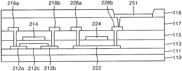
a first transistor which includes a first gate electrode, a first source electrode, a first drain electrode, and a first active layer including an oxide layer, wherein the first gate electrode is on the substrate with the oxide layer therebetween;
a second transistor which includes a second gate electrode, a silicon layer, a second source electrode, and a second drain electrode wherein the second gate electrode is on the substrate with the silicon layer therebetween, and each of the second source electrode and the second drain electrode is disposed on the same layer and includes the same material as the first source electrode and the first drain electrode; and
a light-emitting device including a first electrode, an intermediate layer, and a second electrode,
an intermediate insulation layer covering the oxide layer and the silicon layer, and on which the first source electrode, the first drain electrode, the second source electrode, and the second drain electrode are disposed, wherein
the oxide layer is on the silicon layer.
|