| CPC H01L 29/78642 (2013.01) [H01L 23/5226 (2013.01); H01L 29/41733 (2013.01); H01L 29/42384 (2013.01); H01L 29/4908 (2013.01); H01L 29/66742 (2013.01); H01L 29/78603 (2013.01); H01L 29/78645 (2013.01); H10B 12/05 (2023.02); H10B 12/30 (2023.02)] | 23 Claims |

|
1. A semiconductor device, comprising:
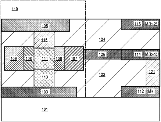
a transistor above a substrate, wherein the transistor includes:
a first metal contact as a source electrode, located in a first metal layer along a first direction;
a second metal contact as a drain electrode, located in a second metal layer along the first direction, in parallel with the first metal contact;
a channel area between a source region and a drain region, the source region adjacent to the source electrode, and the drain region adjacent to the drain electrode;
a third metal contact aligned with the channel area as a first gate electrode, located in a third metal layer along a second direction substantially orthogonal to the first direction, wherein the third metal layer is between the first metal layer and the second metal layer, and wherein one or both of the source electrode or the drain electrode extends laterally beyond the first gate electrode along the first direction; and
a fourth metal contact as a second gate electrode, located in the third metal layer along the second direction in parallel to the first gate electrode, wherein the channel area is between the first gate electrode and the second gate electrode, and wherein the second gate electrode is laterally spaced apart and separate from the first gate electrode; and
an interconnect structure above the substrate, wherein the interconnect structure includes:
a first metal line in the first metal layer, the first metal line laterally spaced apart from the source electrode by an interlayer dielectric (ILD) layer;
a second metal line in the third metal layer, the second metal line laterally spaced apart from the first gate electrode by an etch stop layer; and
a conductive via laterally spaced apart from the source region by the ILD layer, the conductive via directly coupling the first metal line to the second metal line.
|